September 2005
18
M9999-083005
MIC2588/MIC2594
Micrel
PCB Layout Considerations
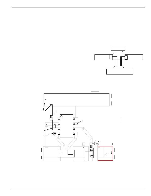
4-Wire Kelvin Sensing
Because of the low value typically required for the sense
resistor, special care must be used to measure accurately
the voltage drop across it. Specically, the measurement
technique across each R
SENSE
must employ 4-wire Kelvin
sensing. This is simply a means of making sure that any
voltage drops in the power traces connecting to the resistors
are not picked up by the signal conductors measuring the
voltages across the sense resistors.
Figure 8 illustrates how to implement 4-wire Kelvin sensing.
As the gure shows, all the high current in the circuit (from
V
EE
through R
SENSE
, and then to the source of the output
MOSFET) ows directly through the power PCB traces
and R
SENSE
. The voltage drop resulting across R
SENSE
is
sampled in such a way that the high currents through the
power traces will not introduce any parasitic voltage drops
in the sense leads. It is recommended to connect the hot
swap controllers sense leads directly to the sense resistors
metalized contact pads.
Other Layout Considerations
Figure 9 is a suggested PCB layout diagram for the MIC2588/
MIC2594. Many hot swap applications will require load currents
of several amperes. Therefore, the power (V
EE
and Return)
trace widths (W) need to be wide enough to allow the current
to ow while the rise in temperature for a given copper plate
(e.g., 1oz. or 2oz.) is kept to a maximum of 10癈 to 25癈.
The return (or power ground) trace should be the same width
as the positive voltage power traces (input/load) and isolated
from any ground and signal planes so that the controllers
power is common mode. Also, these traces should be as
short as possible in order to minimize the IR drops between
the input and the load.
Finally, the use of plated-through vias will be necessary to
make circuit connections to the power, ground and signal
planes of multi-layer PCBs.
R
SENSE
Power Trace
From V
EE
PCB Track Width:
0.03" per Ampere
using 1oz Cu
Power Trace
To MOSFET Source
Signal Trace
to MIC2588/MIC2594 V
EE
Pin
Signal Trace
to MIC2588/MIC2594 SENSE Pin
Note: Each SENSE lead trace shall be
balanced for best performance with equal
length/equal aspect ratio.
R
SENSE
metalized
contact pads
Figure 8. 4-Wire Kelvin Sense Connections for R
SENSE
C
FDBK
R4
*POWER MOSFET
(TO-263)
W
W
W
Via to the
power (VEE output)
plane
Current Flow
from the Load
Current Flow
to the Load
- DRAWING IS NOT TO SCALE-
*See Table 1 for part numbers and vendors
^R1 placed on bottom side
Power Plane -------- (red)
Ground Plane ------- (black)
Trace width (W) guidelines and additional information given in
"P B L
R
mm n
i n "
i n f h
h
Via to the
bottom side
Via to the
ground plane
*SENSE RESISTOR
(WSR-2 or
WSL2512)
D1
MIC2588-2BM
VDD
DRAIN
GATE
OV
VEE
/PWRGD
UV
SENSE
R
FDBK
R3
R2
^R1
C3
Via to the
Return (VDD)
plane
Via to the
power (VEE output)
plane
GROUND
PAD
C1
Via to the
Return (VDD)
plane
Figure 9. Recommended PCB Layout for Sense Resistor, Power MOSFET, Overvoltage/Undervoltage Resistive
Divider Network, and Timer Capacitors
发布紧急采购,3分钟左右您将得到回复。
相关PDF资料
MIC2595R-2BM TR
IC CTRLR HOT SWAP NEG HV 14-SOIC
MIC280-7BM6 TR
IC SUPERVISOR THERMAL SOT23-6
MIC2800-GFSYML TR
IC REG TRPL BUCK/LINEAR 16MLF
MIC281-7BM6 TR
IC SUPERVISOR THERMAL SOT23-6
MIC2810-1JGMYML TR
IC REG TRPL BUCK/LINEAR 16MLF
MIC284-2BMM TR
IC SUPERVISOR THERM 2ZONE 8-MSOP
MIC3385-1.5YHL TR
IC REG DL BCK/LINEAR SYNC 14-MLF
MIC384-1YMM
IC SUPERVISR THERM LOC/REM 8MSOP
相关代理商/技术参数
MIC2594-2YM
功能描述:热插拔功率分布 Negative Voltage Hot-Swap Controller - Lead Free
RoHS:否 制造商:Texas Instruments 产品:Controllers & Switches 电流限制: 电源电压-最大:7 V 电源电压-最小:- 0.3 V 工作温度范围: 功率耗散: 安装风格:SMD/SMT 封装 / 箱体:MSOP-8 封装:Tube
MIC2594-2YM TR
功能描述:热插拔功率分布 Negative Voltage Hot-Swap Controller - Lead Free
RoHS:否 制造商:Texas Instruments 产品:Controllers & Switches 电流限制: 电源电压-最大:7 V 电源电压-最小:- 0.3 V 工作温度范围: 功率耗散: 安装风格:SMD/SMT 封装 / 箱体:MSOP-8 封装:Tube
MIC2594-2YM-TR
功能描述:Hot Swap Controller 1 Channel -48V 8-SOIC 制造商:microchip technology 系列:- 包装:剪切带(CT) 零件状态:停产 类型:热交换控制器 通道数:1 内部开关:无 应用:-48V 特性:故障超时,闭锁故障 可编程特性:限流,压摆率,UVLO 电压 - 电源:-80 V ~ -19 V 电流 - 输出(最大值):- 工作温度:-40°C ~ 85°C 电流 - 电源:3mA 安装类型:表面贴装 封装/外壳:8-SOIC(0.154",3.90mm 宽) 供应商器件封装:8-SOIC 功能引脚:DRAIN,OFF,ON,/PWRGD 标准包装:1
MIC2595-1BM
功能描述:IC CTRLR HOT SWAP NEG HV 14-SOIC RoHS:否 类别:集成电路 (IC) >> PMIC - 热交换 系列:- 产品培训模块:Obsolescence Mitigation Program 标准包装:100 系列:- 类型:热插拔开关 应用:通用 内部开关:是 电流限制:可调 电源电压:9 V ~ 13.2 V 工作温度:-40°C ~ 150°C 安装类型:表面贴装 封装/外壳:10-WFDFN 裸露焊盘 供应商设备封装:10-TDFN-EP(3x3) 包装:管件
MIC2595-1BM TR
功能描述:IC CTRLR HOT SWAP NEG HV 14-SOIC RoHS:否 类别:集成电路 (IC) >> PMIC - 热交换 系列:- 产品培训模块:Obsolescence Mitigation Program 标准包装:100 系列:- 类型:热插拔开关 应用:通用 内部开关:是 电流限制:可调 电源电压:9 V ~ 13.2 V 工作温度:-40°C ~ 150°C 安装类型:表面贴装 封装/外壳:10-WFDFN 裸露焊盘 供应商设备封装:10-TDFN-EP(3x3) 包装:管件
MIC2595-1YM
功能描述:热插拔功率分布 Negative Voltage Hot-Swap Controller - Lead Free
RoHS:否 制造商:Texas Instruments 产品:Controllers & Switches 电流限制: 电源电压-最大:7 V 电源电压-最小:- 0.3 V 工作温度范围: 功率耗散: 安装风格:SMD/SMT 封装 / 箱体:MSOP-8 封装:Tube
MIC2595-1YM TR
功能描述:热插拔功率分布 Negative Voltage Hot-Swap Controller - Lead Free
RoHS:否 制造商:Texas Instruments 产品:Controllers & Switches 电流限制: 电源电压-最大:7 V 电源电压-最小:- 0.3 V 工作温度范围: 功率耗散: 安装风格:SMD/SMT 封装 / 箱体:MSOP-8 封装:Tube
MIC2595-1YM-TR
功能描述:Hot Swap Controller, Sequencer 1 Channel -48V 14-SOIC 制造商:microchip technology 系列:- 包装:剪切带(CT) 零件状态:停产 类型:热交换控制器,序列发生器 通道数:1 内部开关:无 应用:-48V 特性:闭锁故障 可编程特性:限流,故障超时,UVLO 电压 - 电源:-80 V ~ -19 V 电流 - 输出(最大值):- 工作温度:-40°C ~ 85°C 电流 - 电源:4mA 安装类型:表面贴装 封装/外壳:14-SOIC(0.154",3.90mm 宽) 供应商器件封装:14-SOIC 功能引脚:CFILTER,CNLD,DRAIN,PGTIMER,OFF,ON,PWRGD1,PWRGD2,PWRGD3 标准包装:1
